I have spotted what I believe are several errors in the published schematic for the RAK13302 (RAK13302 WisBlock LPWAN Wireless Module VC Datasheet)
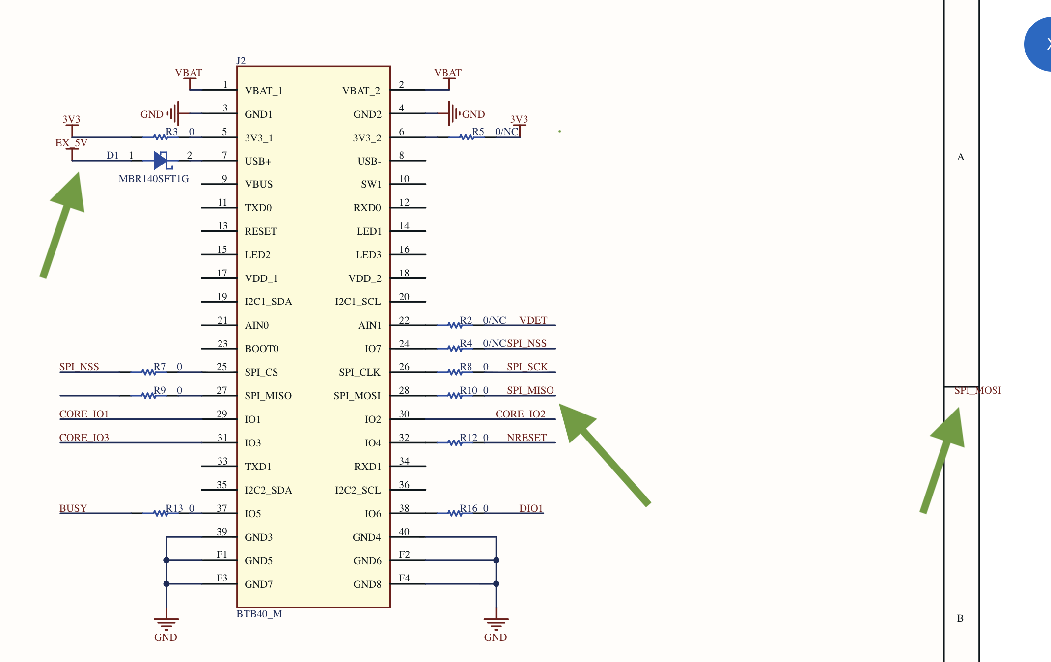
The leftmost arrow shows that the external 5V rail is connected to USB+, a 3.3V data line.
The next arrow shows SPI_MISO being connected to SPI_MOSI.
The last errors shows that the SPI_MOSI net label is off in the margin and it’s unclear what it’s supposed to be labeling.
Can I assume the actual board has MOSI connected to MOSI, MISO connected to MISO and EX_5V connected to VBUS?
Thank you.