I’m laying out a custom PCB that will incorporate the RAK4200 Module. I have several questions about the module pin descriptions found in the device documentation and need these questions answered before I can finish this effort:
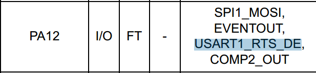
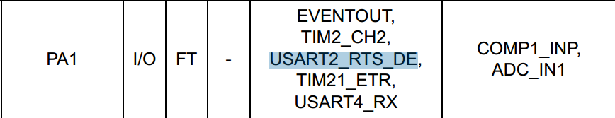
There are two sets of UART interfaces with pin names: RX, TX, and DE. The name of the two DE pins implies they are the “Driver Enable” output pins (used for RS485 hardware flow control). However, these same pins can also be re-assigned within the module’s firmware to operate as the RTS hardware flow control mechanism managed when RS232 protocol is used. Since this modules is using RS232, are these two DE pin (module pins: 3 and 6), used as RTS output pins?
As I noted above, there are two UART interfaces found on the RAK4200 module. The first (module pins: 1-3), implies this is the “main” UART interface. I’m assuming this is the UART interface where AT commands are processed. My questions is, what is the purpose of the second set of UART pins (module pins: 4-6)?
Looking at the schematic of the RAK4200 module, it appears the SPI bus pins (module pins: 15-17) are connected to an internal bus of the RAK4200 module. It is used to connect the STM32L071 to the SX1276 transceiver. Is there any advantage to my design if I bring these pins out to my host MCU? I do not see any advantage to doing this. I am already going to bring out the SW debugging lines (module pins: 7 and 8), to a header for programming/upgrading of the RAK4200. If no advantage, I will leave these pins unconnected.
The I2C bus lines (module pins: 9 and 10) appear to have no purpose. Unless the source code for the STM32L071 is provided, I don’t see any purpose to connecting these pins. Is there any plan to make the STM32L071 source code available so these pins could be used by my application? If not, I will leave these pins unconnected and assume the STM32L071 will keep these in a low power, tri-state configuration.
Finally, I don’t see an explicit “module enable” input control line. I assume the module will enter a “deep sleep” (STM32L0 ultra-low power consumption), when my host processor “closes” the main UART interface. In other words, when the host processor drops the logic level of the RAK4200 module’s main RX pin (module pin: 1) to a “low” level. Conversely, to wake the module back up, the wake-up trigger is the rising edge of this same pin (as it will drive the “idle” condition on the UART RX pin). Is this correct? If not, can you explain the mechanism to force the module into the “deep sleep” state and how to wake it up?
You can use one UART interface as comunication port to set some AT commands and the other one can be used as the data communication interface to communicate with other modules. It can also be defined as an ordinary IO port
It is better to leave these pins unconnected if you don’t need it.
If you don’t need I2C you can leave them unconnected.
You can turn off UART controller before sleep, set RX pin to input mode of built-in pull-down, and then set external interrupt of rising edge. If UART has data, it can wake up
Thank you for the quick reply. All of your answers have been very helpful, except the last one (I just need some more clarification). Thus, I would like to describe my use case better.
I’m using the RAK4200 module as a “modem”. My application requires a fairly large CPU with floating point capability. So my host MCU (an STM32L4xx) will require the ability to wake up the RAK4200 module when my host MCU requires transceiver services (i.e. LoRa network connectivity) from the RAK4200 module. Thus, after the RAK4200 module is commanded into a power saving mode using an AT “sleep” command (issue by my STM32L4xx host MCU), I need a mechanism to wake the RAK4200.
I know I can reset the entire RAK4200 module by driving input pin MCU_NRST (module pin: 18) momentarily low. But I would like to avoid this as it will force an MCU reset on the STM32L071 (and consume power as it has to re-execute all of the STM32L071 initialization code as well as recharge all of the filter capacitors). Is this the only way to wake up the RAK4200, is by forcing a full module reset?
Finally, if I understand your answer to my original question 5, it sounds like the RAK4200 can be used as a wake-up source for my host MCU. Thus, I could place my host MCU into a very low power saving mode and wait for the module to wake it if the RAK4200 needs to be “serviced” by my application running on the host MCU. Is this correct?
I’m only familiar with Class A LoRa so I was surprised to learn of this capability (where the RAK4200 can wake up and alert my host MCU). I’m assuming this capability is provided to allow Class B or C downstream message, sent by a gateway (and received by the module), a mechanism to notify the host processor that the module has data, or needs to be serviced.