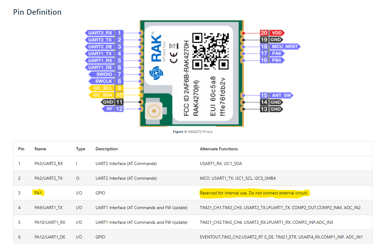
The datasheet for the RAK4270 shows pins PA1 (Pin 3) and PB4 (Pin 16) reserved for internal use, but the schematic shows them not being used for anything.
I would like to use these pins for my application. Is there any problem with using them? I am writing my own firmware for the module, so I am not using the AT-Command or the RUI firmware.
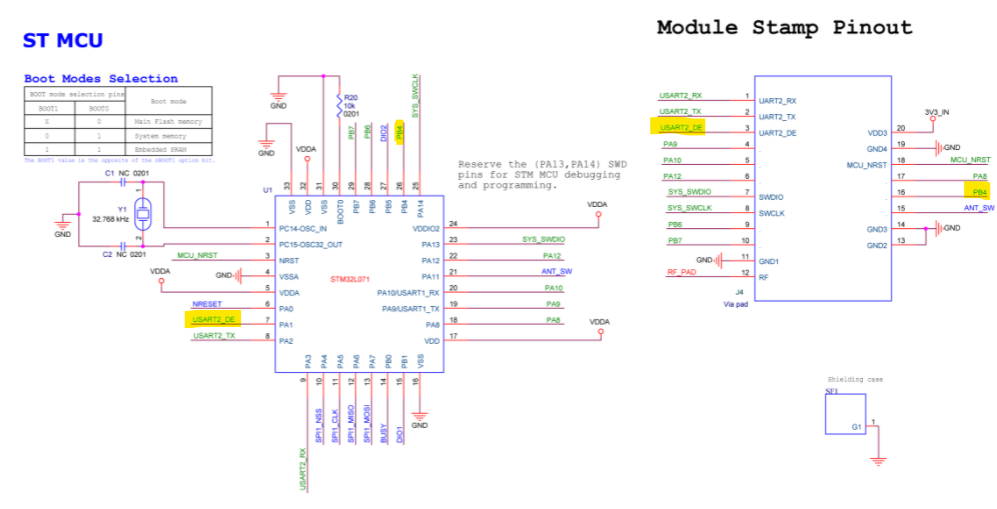
These two pins are the SWD interface for flashing and debugging the device with a Segger J-Link or DAPLink RAKDAP1.
If you do not use SWD to flash or debug the module you can use them in your application.
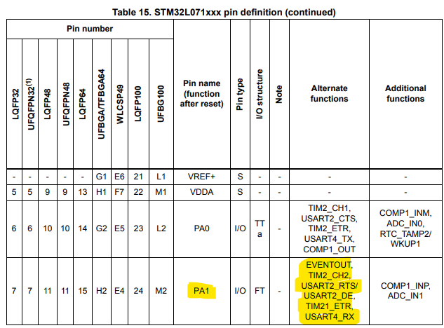
Further, the description for PA12 in the RAK4270 alternate function description in the screenshot above is actually for PA1 according to the STM32L071 datasheet:
This leads me to believe that my concerns could all be due to errors in the RAK4270 datasheet.