Hi RAK Team / Community,
I’m designing a PCB with a RAK4630 module powered by a coin cell through a TPS61094 regulator. I want to make sure my power and RF layout is correct before I proceed. Here’s my current plan and the questions I have:
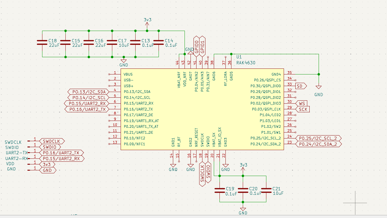
![]() Power Setup
Power Setup
Coin cell → TPS61094 regulator → 3.3 V rail
VDD_NRF connected to 3.3 V
VBAT pins: VBAT_NRF, VBAT_SX, VBAT_IO_SX all tied to VDD_NRF (single-rail design)
Decoupling capacitors (all 0402):
| Pin | Capacitors |
|---|---|
| VDD_NRF | 0.1 µF + 10 µF + 3×22 µF |
| VBAT_NRF | 0.1 µF |
| VBAT_SX | 0.1 µF + 10 µF |
| VBAT_IO-SX | 0.1 µF |
Questions:
- Is it correct to tie all VBAT pins to VDD_NRF in a single-rail coin-cell setup?
- Are the decoupling caps sufficient for LoRa TX bursts (~100–150 mA)?
- Any concern about additional caps affecting coin-cell current draw or module operation?
 RF Pins
RF-LORA and RF-BT pins **left as they are on the module
Plan to use an external antenna via the onboard U.FL port
Questions:
4. Can I leave the RF pins as is, since the module already has internal matching and routing?
5. Any recommendations for connecting the external antenna to maintain proper RF performance?