
I’m trying to run my working FW that runs on the WL Nucelo on the RAK3172-E after I modified it to fit the WLE5
My first goal is to see the join requests that are sent from the device on the RAK GW LoRa Packet Logger.
I don’t see anything there.
What might be the problem?
I tried to use another RAK3172-E with its out of the box FW and I issue AT+JOIN but again nothing on the logger
Logs of module when you send the AT+JOIN with original fw ? and what happens with your own code ? have you checked it really sends the Join command ?
Did you check also on Lora server on which your gw is connected ? Your gw is working well with other Lora devices ?
AT+JOIN
OK
+EVT:JOIN_FAILED_RX_TIMEOUT
My FW runs and joined successfully on the Nucleo and the GW logger display all the interaction as expected.
The LNS is not in the game if I only look for the join request on the GW logger, if it is not there it will never get to the LNS
I think you are wrong there ![]() From logs you posted it looks like your device sends the join command but never received the ACK from Lora network. Don’t forget also (excepted if you are in middle of desert) that join message sent by your device might be received by an other gw around
From logs you posted it looks like your device sends the join command but never received the ACK from Lora network. Don’t forget also (excepted if you are in middle of desert) that join message sent by your device might be received by an other gw around ![]()
Are you sure the antenna on the device is properly plugged and for the frequencies used ?
I’m sure I’m not wrong 
I think you are not understanding my question 
If the join request does not reflect on the GW logger then no connection to server will be attempted and thus no ACK will be received
Hi @EGmbed ,
It seems related to RF (SW or HW). What is the frequency of operation of both device? A SDR is handy on this kind of situation to see if the device is really transmitting. Also, if another device connects successfully to the gateway, we can focus on the device side.
Hi and thank you for answering.
I’m working in 915 band.
The GW is receiving and transmitting from\to my other (many) devices on this band (915)
I am using RAK3172 at US915 a lot. Maybe we can check the antenna? Also is the mask set correctly? Usually it should be AT+MASK=0002 on most LNS. How far is the device from the gateway?
Thank you Carl, the mask did the change indeed and I can see the transmission on the GW logger.
I’ll continue tomorrow to try and join the LNS and I’ll be in touch
Hello Carl,
Now, After I see that the RAK3172-E with its original FW is communicate with the GW I want to use my STM32WL-Nucleo FW to do the same on the RAK3172-E.
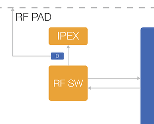
For that I need to adjust the FW to fit the 3172 HW connections, as I see it the only thing I need to do is to set the RF Switch, currently, in my Nucleo setup, it is set like this:
- FE_CNTRL1: PC4
- FE_CTRL2: PC5
- FE_CTRL3(VCC): PC3
Can you please explain how it is connected on the 3172?
Hi @EGmbed ,
I am not sure if you already see this guide but this can help you port the RAK3172 to STM32CubeIDE. It is based on the examples of the STM32WL SDK for the Nucleo eval board.
You can get the necessary changes on the RF Front End control on the Radio files in the low level development folder here. This is also on the guide I shared above.
Hello Carl,
I tried to follow the guide you pointed me to but I was not able to run my application that is working on my target that is based on the STM32WLE5.
I’m working with CubeIDE and with STM32WL SDK and this is how I build and debug the application on my target that as I mention is based on the STM32WLE5.
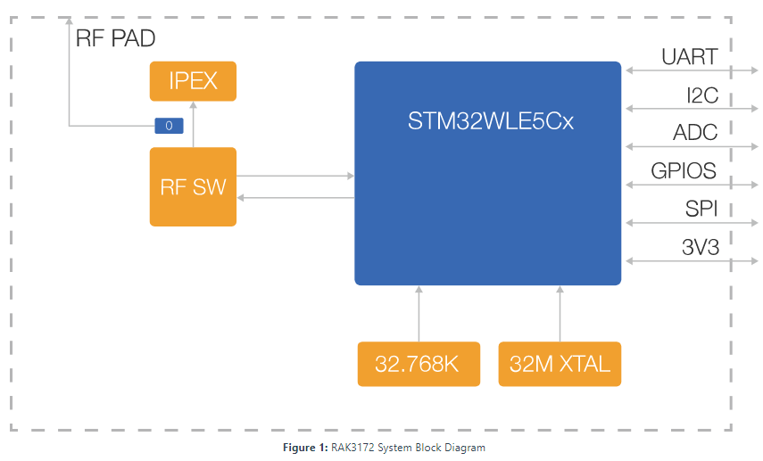
Can you please send me the schematics on how the STM32WLE5 is connected to the output pins RF switch on the RAK3172?
That way I can change the GPIOs on my application and adopt it to the RAK and test it.
Thanks,
Eyal
On the RF source files I shared, you should be able to see the pins used on the RF related IO pins. If you still need that specific section on schematic, I will send it to your inbox here in RAK forum.
Thank Carl but I prefer not to do reverse engineering from a code I was not able to run and if I can see the section in the schematics where the lines that are related to the RF switch (As I wrote above) it will be better.
I assume that other then those lines all the other lines (GPIOs, UARTs etc.) are as it documented here:

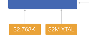
I would like also to see to where the clocks are connected in order to make sure it is the same as I use in my code:
Thanks,
Eyal