We turned the unit on and off about 50 times - the consumption of the unit is about 9 mA. Everything works as normal for us.
Then we connected to the RAK3172-SiP via the SWD interface (we tried the STLINK v2 mini adapter and the STM32 ST-LINK Utility) and looked at the data in the internal memory (there is the factory firmware).
Then we disconnected the SWD interface and reset the power supply of the 3.3V block.
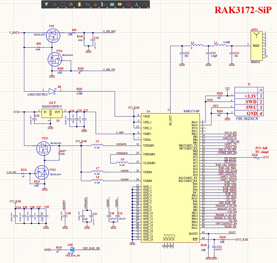
After re-powering our block began to consume abnormal current. During the analysis it was found that the resistance relative to GND of the VDDRF and VDDPA circuits is not more than 4 ohms.
We disconnected power from the VDDRF and VDDPA circuits. After applying power, the consumption of the module was 9 mA and about 3 mA when the RAK3172-SiP was put into reset.
We installed a new RAK3172-SiP into our board and repeated the experiment - the result was similar - a breakdown to GND on the VDDRF and VDDPA circuits.
Can you give us an idea what could be wrong? Thanks in advance.
After setting the jumpers E1,E2 and E3 (L5, L7, L8 in my schematic) and connecting to the module via SWD we got the same result - a breakdown between GND and VDDPA, VDDRF.
Our hypothesis is that when you connect to the processor via SWD and try to read data or flash our firmware, the STM pins that control the radio part are in Z state and this causes power failures on the VDDRF and VDDPA circuits. What do you think about this, or do you still think that the VDDSMPS, VDDRF and VDDPA circuits should have strictly ferrite beads? Then what about your examples of power organization in the application on the site, where these circuits are directly connected to the VDD?
As you say, this happens after you connect the STLink over SWD, I have two follow up questions.
a) Are you using a custom firmware, if yes, is the firmware based on our RUI3 API?
b) Beside of “looking at the data in flash” are you doing anything else through SWD? Are you flashing your own firmware or are you debugging the code?
I am not familiar with the STLink, but you are connecting the 3V3 of the SWD interface to the 3V3 volt of the board. Is the 3V3 on the STLink supplying 3.3V or is it a reference voltage input?
I don’t understand as well your power supply connections.
In the schematic you are connecting VBat (what voltage is there) to 3V3_RAK. But 3V3_RAK is as well supplied from 3V3 if 3V3_EN is enabled. Unless there is something that is not shown on that part of the schematics, there could be a conflict if V_BAT is higher than 3V3.
Another thing, you are pulling SWD to 3V3, but if 3.3V_EN is off and V_BAT is not connected, the RAK3172-SiP is powered down but the pin is still pulled up. Same for GPIO PC0.
a) At the time of the ST LINK connection we are not yet uploading our firmware to the RAK3172. It still has its factory firmware inside.
c) We only connect the SWD interface to the RAK3172. Once connected we see the contents of the internal flash memory of the RAK3172. Next we disconnect from the RAK3172. We do not do any debugging or flashing of our firmware via ST LINK.
About ST LINK - The 3V3 on the STLink is a 3.3V power supply.
Regarding the power supply of the unit.
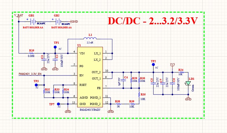
The entire unit is powered by two AA batteries in series. The power range of the batteries will be from 2 to 3.2 V maximum.
So the 3V3_RAK circuit will always be powered by the battery minus the D8 diode drop (about 0.3-0.4 V)
When the other scheme peripherals need to be powered up, after coming out of power saving mode, the RAK3172 controller turns on a 3.3V power supply. When the 3.3V supply is turned on, the 3V3_RAK circuit is stable at 3.3V. Since the 3.3 V circuit voltage is always greater than the battery voltage, there is no conflict between the two because of the presence of diode D8
Could you see my answers to your questions? Maybe you have some ideas about our problem (RAK3172) with VDDRF power shorting (resistance between VDDRF and GND is about 15 ohms) in the controller when connecting/disconnecting the programmer via SWD.
I did try to replicate your situation. I used a RAK3272-SiP breakout board connected to 3.3v power supply. The beads E1 and E2 are connected to VDDRF an VDDPA pins. After more than 50 times of supply voltage connect and disconnect. I connected it to STLINK then tried to read, erase and write the latest RUI3 firmware for RAK3172-SiP. The VDDRF and VDDPA pins are still working ok.
I only have basic connections to the breakout board.
I am leaning towards the hw/circuit that causes the issue and not the STLlink.
If you disconnect the RAK3172-SiP, is the low resistance on VDDRF and VDDPA still present?
Do you have a RAK3272-SiP breakout board where you can possible perform same test?
Btw, I am not sure if disconnecting VDDRF and VDDPA supply is a good idea. Do you have some reference on this approach? I haven’t looked deeply on the internals of STM32WL chip power rails but I haven’t seen design suggestions to disconnect those power pins to save battery life. Maybe for a simple test (same as the breakout board), we can create a solid 3.3V supply to all power pins (no disconnect via mosfet) then do the test again? Also, if you can disable the boost section as well and just supply external stable 3.3V to do the voltage supply cycling test? This way we can isolate on which part of the circuit that causes the issue. As we know, based on the information you gave, at 50 switching on and off cycle, the issue occurs. There could be some spike or some kind of noise during that switching that causes the damage on the VDDRF and VDDPA lines.
One remark about your power supply design from our R&D engineer:
One thing we have to consider:There is a 33uH inductor between 3V3_RAK and VDDPA(Also between 3V3_RAK and VDDRF).When power down,there will be a high voltage spike which will damage VDDPA and VDDRF.
It’s easy to catch this spike by oscilloscope.
You might need to check the logic of your power supply.
We cannot reproduce your problem and as Carl suggested you might want to check your circuit, maybe measuring the voltage with an oscilloscope at VDDRF and VDDPA an check whether you can see any voltage spikes there while you are switching on and off the supply.