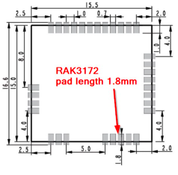
I’m creating a PCB footprint for the RAK3172. During this effort, I realized the datasheet fails to show the complete footprint dimension for the recommended pads.
I can see the width of each pad is recommended to be 0.7mm. I can also see each pad should extend 0.8mm beyond the package dimension. But the “total” pad length can NOT be determined with the given layout drawings.
I need to know how long you recommend the pad should be under the package (or the total length of the pad).
Please use this drawing for the length of the pad. It should be 1.8mm. It still depends on you if you want to make it a bit longer if you are hand-soldering some prototypes. The docs will be updated after the Lunar New Year holiday.