It would be useful to see the top copper layer as a ground plane there will have much stronger coupling to the module.
I am really trying to understand as much as possible about the potential issue as we are sitting on several thousand dollars of boards that may get scrapped.
Unless your measuring the TX RF power with an RF power meter or a spectrum analyzer your assumption are rather presumptive. If your setting the TX RF power to +22 dBm then you should see this on the instrument. You can also conclude that if the TX chain is as expected then the RX chain will work as expected.
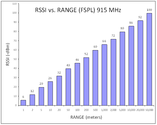
Another way without instruments is to use the path loss equation and plugging-in the variable, such as antenna gain (Gt, Gr), distance (D), TX RF power.
20 LOG(D) + 20 LOG(f) + 20 LOG (4 PI / c) - Gt - Gr.
If the RSSI reading is what the equation predicts then you know it’s 100% its working.
This graphs shows you the expected RSSI.
Antenna gain = 2dBi
F = 915MHz
TX PWR = +22 dBm
I agree that my preliminary tests are presumptive. Their purpose was a first-pass evaluation of some antennas.
But anything resembling the 40dB reduction in transmit power that was originally reported should have been clearly evident, presuming the NUCLEO board wasn’t similarly affected.
It would have been useful to test my board with the NUCLEO’s antenna as well - something that will happen when I find the appropriate pigtail.
At this point, I am satisfied that there is not an issue with the stock of modules I have on hand.
However, this doesn’t discount that @frank_r actually has a problem.
I would like to pose a thought which might lead to another conclusion. I won’t defend this thought as I simply don’t know.
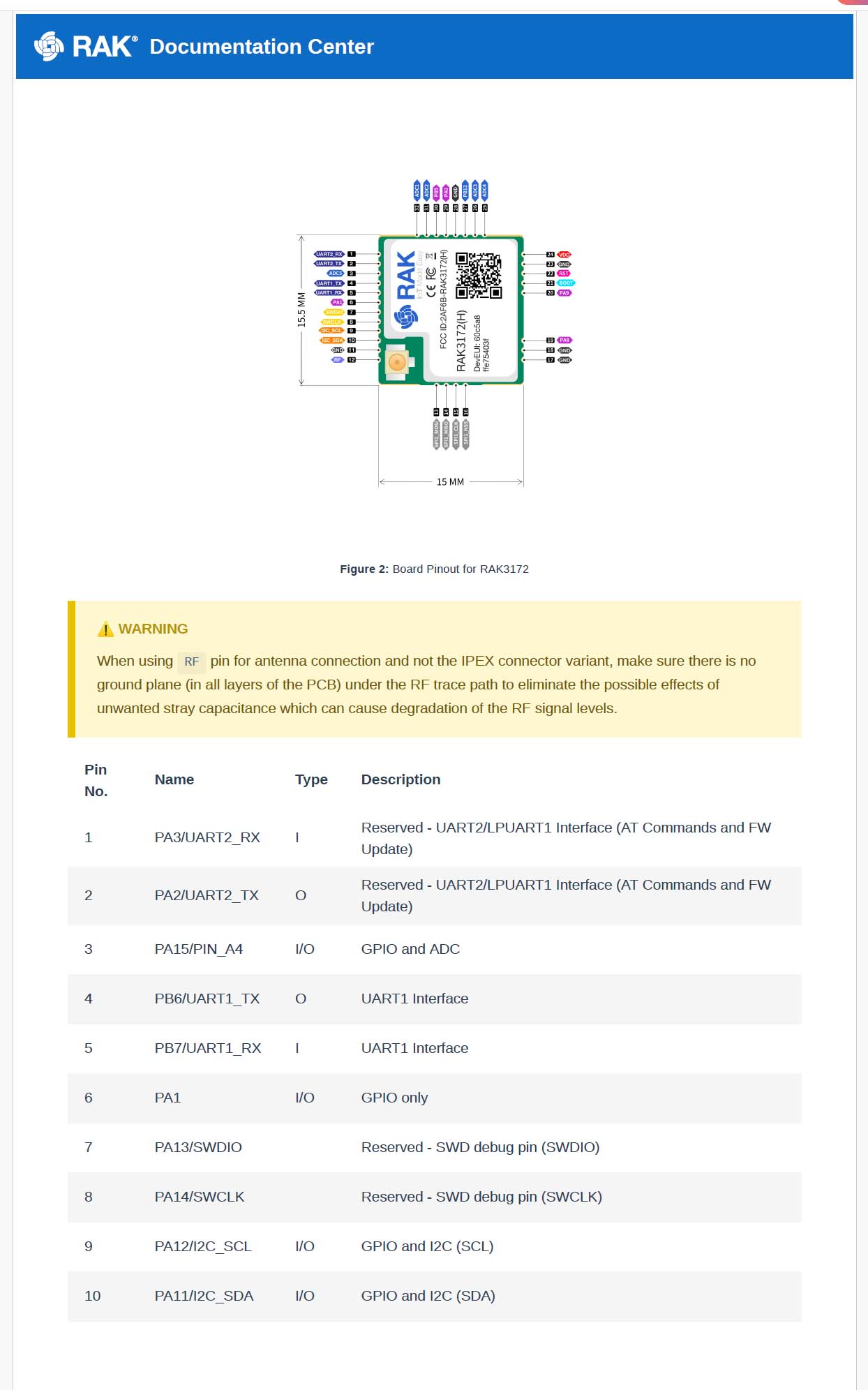
There are two versions of the RAK3172 in respect to range (high freq., low freq.). The RUI3 firmware determines which version based on whether the pin PB12 is tied high or low.
I don’t use RUI3 and I can only guess what is happening under the hood with the RAK3172 itself.
If the low frequency module version uses the “low power” Tx pin (max +14dBm) while the high frequency version uses the “high power” Tx pin on the STM32WL chip, then this scenario may play out…
Pin 27 of the module is PB12. If this were accidentally tied to ground, this might force the RUI3 firmware to treat the module as the wrong type and not enable the PA for the “high power” Tx pin.
I avoid using this pin completely and leave it floating in my design.
However, Frank’s original PCB snippet shows a net connected to pin 27.
Is it possible that this connection to pin 27/PB12 is overriding the hardware type to the firmware and resulting in incorrect transmitter configuration?
The idea could be complete rubbish.
Feel free to ignore. As I said - I won’t spend time defending the suggestion.
I was the having the same TX RF power on two batches 2 years apart. It seems unlike the RAK would have changed the layout of the RAK3172 module since introduction?
Yes indeed I was having some issue with PB12 (pin 27) and tied it high with a jumper. Some modules worked when left floating and some didn’t. Really I don’t understand the point of this pin. The firmware should recognize what frequency is sent and adjust its itself accordingly.
Another user reported a problem with TX RF power, I’m not the only one.
When I first detected this problem, the PCB had copper removed under pin 12 except the bottom layer 61 mils away (as recommended in the spec). By removing the module and reinstalled a new module without pin 12 connected the TX RF power returned to normal. On another board with 2 RAK3172 modules I completely removed all copper under all the layers under the RF output section. The board never had any problems.
The difference between low frequency (433/470 MHZ) and high frequency (860/915MHz) variants are not only the PB12 pin. There is a difference in the RF path matching circuit between the two variants.
So it is not only the frequency the firmware is setting. It has to match with the RF path matching circuit or you will get bad RF performance.
Bernd, apart from the change in the matching network between the different bands, are you also switching between using RFO_HP and RFO_LP pins on the chip itself?
Hi Bernd (and other’s interested) … Just wondering where this left off. Now, a few months later, I have a design that I’m about to manufacture.
In my design I wish to accommodate both the connectorized and unconnectorized module variants so I have an engineered 50 Ω trace from pin 12 to a pi network and it includes a small 0402 0 Ω removable connection very close to pin 12. The 0 Ω resistor can be removed when using the u.fl connector model.
So in summary, in my case I have an engineered 50 Ω trace from pin 12 that can be disconnected when the user chooses to use the module with the u.fl connector. I have no special removal of copper layers…
So I seek any insights that might lead me to change the design. Specifically: In the end of this discussion was it determined that no special removal of copper layers is required and, have I missed something …
I would go a bit further and remove a larger area under the RF section, as indicated above. I have built a PCB with this approach and it works very well. In your case connect the 0 ohms resistor to pin 12 with the GND to pin 11 for the 50ohms RF path with a trace that surrounds the area.
Thanks for this. I’ll take your advice and make the change on my board. Experience speaks here! I’d really like to see the Gerber files but I won’t ask for proprietary stuff.
Interestingly RAK has changed the yellow warning box and removed the specific warning and replaced it (see here).
This issue caused me a lot of problems. My RF output was down over 40dB. A temp. fix was to remove the module and resolder it with no connection from pin 12 to the PCB. and making sure pin 12 did not touch the PCB. This fixed the problem. My next version of the PCB removed pin 12 altogether and cleared the copper as indicated under the module. There is an issue with the RF output on this module. Its extremely sensitive to output matching and termination from pin 12… A more robust RF output would be desirable.
It’s very strange that the RF output could be affected to this extent (-40dB) with a GND plane under pin 12. It’s almost as if the U.FL RF connector was turned off on purpose if the module detects a load on pin 12. This sounds like a plausible explanation. What is the output structure of the module? Does the module looks for a load on pin 12? Perhaps the load detect circuit needs to be examined.
Please note that the warning was changed because the behavior cannot be generalized to all designs. We added new notes which can be considered in most designs but the ground plane removal is still case to case basis (proven that it does not always give bad effect on RF performance).
The 40dB RF attenuation resulted in a range of less than 100m!!! RAKWireless needs to disclose the RF output structure. From the RF output behavior it seems that the RF signal exist either on the U.FL connector or Pin 12 but not both at the same time. The circuit that detects and does the switching is temperamental. Sometimes it works and sometimes it doesn’t. This is an issue that is not going away.