I know this question has been asked and answered, however, I am still having some trouble understanding how I should set up my power.
For my application, I am using an external watchdog IC (TLP5010) to “wake-up” my 3.3V regulator (TPS63051) which then would power on the RAK4630 chip. The EN pin of the regulator is tied to a three input OR-gate, one input from the pulse of the watchdog, one input from the RAK4630 itself so it can keep itself on longer than the pulse by using a GPIO pin, and a jumper which allows it to be tied to battery voltage to force it to stay on during programming and debugging.
The timer circuit works exactly as intended, however, I noticed that even in “timer” mode, the MCU stays on and functional when I expected it to be turned off. I tied VBUS to USB voltage (not plugged in during this test), VBAT_NRF to the battery votlage (14500 Li-Ion battery), and all other voltages to the regulated 3.3V from the regulator. As a test to make sure it was not firmware related, I uploaded Meshtastic, and that worked totally fine regardless of if the regulator power good pin was high or not.
I tested my regulator and although the EN pin was low and the PG pin was low, there was still 3.3V on the output. I am not 100% sure if it was drawing current from the supply or not, but
I wanted to double check and see if I misunderstood:
Does the RAK4630 stay on and powered purely from the VBAT pin, or is my regulator just staying on and awake when it shouldn’t?
If the answer to the first question is yes, is there a way I can prevent the RAK from being on and active at all until the 3.3V regulator is on and functional?
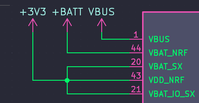
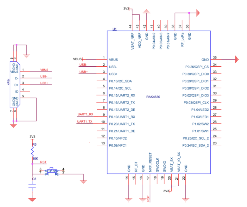
The default configuration of nRF5840 in RAK4630 is high-voltage mode. This means that the VDD supply is coming from VDDH (this is connected to VBAT_NRF).
You should not put 3.3V to VDD_NRF since it is already supplied by the VBAT_NRF.
To completely turn of the RAK4630, you have to remove both +3.3v and +Batt.
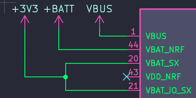
There is another option you can do which operate the nRF52840 in normal mode. I highly suggest you backtrack the discussion here - RAK4631 without baseboard
In normal mode, it will allow you to connect all supply in 3.3v voltage rail. No need to get bothered by the VBAT_NRF.
However, in your case, since you are developing custom PCB, it might be a good option too if you can switch from high-voltage mode to normal mode via jumpers/pad/resistor. Like on the design of RAK4630.
This resistor will allow you to switch from high voltage mode to normal mode depending on how and where the VBAT_NRF and VDD_NRF pins are connected. I think this is a more flexible approach and will be helpful on the proto stage of the design.
What you see is correct. I am working on the documentation update so we can show both Normal Mode and High Voltage Mode on the RAK4630 Quick Start Guide. Your basic circuit for normal mode should look like this.
Do you have, or know where I could find, power requirements for the SX chip? I’m specifically looking for voltage ripple recommendations. For example, what is the maximum voltage ripple that is considered acceptable for SX input (to ensure it’s not causing problems with RF emissions)? This info has been particularly difficult to track down.
I’ve checked the datasheet and I didn’t see any voltage ripple requirements in Vbat. Likely the reason is that there is still LDO and DCDC section inside the transceiver than regulate the input Vbat. The only way to know if the supply input ripple is ok is if it is tested in actual.
I’m sorry, I was asking about input voltage to the SX1262. Thanks for your time with my questions.
May I ask if your HW engineers have a ballpark voltage ripple they try to achieve for RAK power circuits feeding into the SX1262? Do they have a maximum ripple they try to stay under?
I’m really just looking for a rule of thumb when designing power circuits for transceivers like the SX1262. This type of information has been really hard to find. The datasheets are always like “the input voltage ripple should be as low as possible” which isn’t very helpful when you’re starting out. Are we talking in the range of 100mVpp? 50mVpp? 10mVpp?
I have to check with the team about this. To make it clear, you need this info to ensure good RF emission right? RF emission means (1) for EMC compliance or (2) RF emission like RF signal propagation?
Also this voltage ripple is the input voltage to Vbat of SX1262 right? Not the voltage ripple generated by the internal DC/DC of SX1262?
Yes, for good RF emissions. Primarily to ensure good RF signal propagation.
Yes, I’m talking about the voltage input to the SX1262 from my external power circuit (like on a custom base board). Yes, my supply to VBat of the SX1262
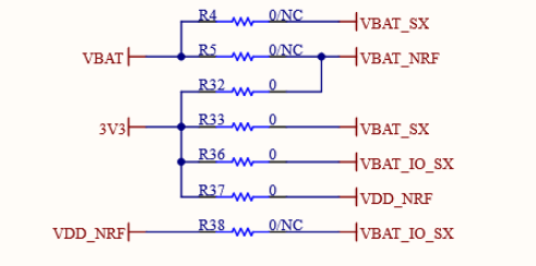
Just for information, you can connect all together (except VUSB)
That’s what’s done with official NRF52840 dongle, I’ve made some test, if you plan to run on 3.3V up to 3.6V you can connect this power to all following pins:
VBAT_SX
VBAT_IO_SX
VDD_NRF
VBAT_NRF
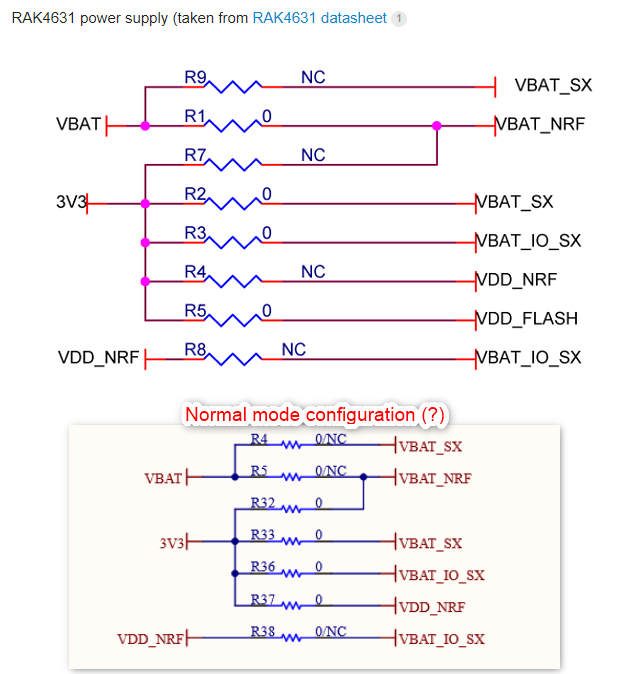
It’s absolutely no problem, check this out
Using this design, we are about 5uA sleep mode on RAK4630 on our custom PCB.
Dual eyes pair are always better then one, if someone could confirm what I’ve done, would be awesome
Thank you for sharing this @Charles . You always have valuable insights that are helpful to many users
I haven’t looked deeply on nRF52840 but it could be that there is some kind of comparator internally that automatically switch the power mode of the chip. Very user friendly since no special register configuration is needed.
Yeah I did also some testing with internal regulator REG0 / REG1 enabled or not (in this wiring configuration) to see influence on power consumption, and I came to the same view, nrf52840 is smart enough to auto adapt internal regulators in this case because changing values had no incidence on consumption.